


Integrated circuits (ICs) are fundamental components found in virtually every electronic device. They consist of numerous discrete elements integrated onto a compact silicon chip.
As technology progresses, IC designs become increasingly complex. This growing complexity makes precise pin inspection essential to ensure compliance with strict quality control standards.
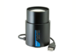
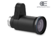
For high-precision inspection applications, Vico Imaging’s COOLENS® Bi-Telecentric lenses are widely used to achieve accurate IC pin inspection results.
PCB manufacturers typically rely on datasheets and technical documentation to understand pin configurations and complete circuit connections. However, even minor pin misalignment or incorrect connections can lead to circuit failure.
For this reason, optical inspection has become a critical step across various manufacturing stages. A clear example of this can be seen in the production of IC sockets.
To ensure that each IC pin functions correctly, visual inspection is necessary. In addition, advanced solutions such as Automated Optical Inspection (AOI) enable highly accurate and efficient pin verification.
This article explains the importance of IC pin inspection and highlights how modern technologies—such as bi-telecentric lenses—enhance inspection accuracy.
What is IC pin inspection?

IC pin inspection is a process used to verify the integrity of electrical connections between two or more points within an IC package. The goal is to identify defects, inconsistencies, or irregularities.
This process typically involves examining pins with specialized equipment such as microscopes or precision lenses, ensuring that their physical properties match datasheet specifications.
Pin inspection helps detect wear, deformation, or damage that might otherwise go unnoticed during assembly—issues that could result in reduced performance or complete IC failure.
Common causes of IC failure include manufacturing defects, physical damage, electrostatic discharge (ESD), and extreme operating conditions. Pin-related issues are also a significant risk factor.
By implementing thorough pin inspection procedures, manufacturers can detect defects early, maintain product quality, and ensure compliance with industry standards. Regular inspections also help prevent costly production issues.
Beyond manual inspection, many manufacturers use Automated Optical Inspection (AOI), which employs industrial cameras to capture detailed images. Image processing software then analyzes these images to confirm that soldered pins meet design specifications. This approach reduces human error and increases efficiency.

Common IC pin inspection methods
Different inspection techniques are used depending on the IC’s complexity and application.
- Manual visual inspection
For simpler ICs, trained operators may perform inspections using magnifying tools or microscopes. - Automated optical inspection (AOI)
AOI systems are suitable for both simple and complex ICs, offering faster and more accurate inspection than manual methods.

X-Ray inspection
X-ray inspection is one of the most advanced methods, particularly effective for BGAs (Ball Grid Arrays).
This technique directs X-rays through the PCB. Denser materials, such as solder joints, absorb more radiation and appear darker in the resulting image. A detector converts the X-rays into visible images for analysis.
X-ray inspection is highly effective for identifying solder bridges, excess solder, hidden defects, and structural inconsistencies. It is also widely used for through-hole inspection, surface-mount analysis, and lead-free solder evaluation.
Optical inspection

Optical inspection involves using imaging systems to evaluate IC pins. Historically, this relied on manual observation, which was prone to errors.
Today, advanced tools such as bi-telecentric lenses significantly improve inspection performance. These lenses are ideal for examining small components with high precision, especially in confined spaces.
A typical system includes a high-resolution camera, a magnification lens, and a display interface. Combined with image processing software, this setup enables accurate measurement and defect detection.
Technicians can inspect outer pin rows visually, and with proper lighting, even inner rows can be analyzed. Common detectable defects include:
- Irregular solder joint shapes
- Surface inconsistencies
- Bent or misaligned pins
- Contamination or debris
Optical inspection is highly effective in identifying open circuits, short circuits, corrosion, and discoloration.

Electrical testing
Electrical testing evaluates the functional performance of a PCB by passing current through it to detect faults such as shorts or open circuits.
Unlike mechanical stress testing, this method focuses on electrical stability. However, it does not provide precise defect localization—especially for pin-related issues.
While electrical testing is important, it is generally less effective than optical inspection for identifying physical pin defects.
Equipment required for visual IC inspection
Accurate IC pin inspection requires not only precision but also a well-designed machine vision setup, typically consisting of:
- Computer system
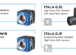
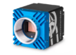
- Industrial camera with bi-telecentric lens
- LED ring light
- Diffuser
Lens
In modern electronics manufacturing, staying competitive requires advanced imaging tools. Bi-telecentric lenses offer significant advantages, particularly in improving image resolution and measurement accuracy.
VicoImaging develops industrial lenses designed to meet strict industry requirements. Their bi-telecentric lens models are optimized specifically for IC pin inspection, offering ease of use and minimal setup time.


Camera
The inspection system typically includes a high-speed industrial camera with the following characteristics:
- Stable data transmission
- High image quality
- Fast image acquisition
- Automated detection capability
Light source
Lighting plays a crucial role in inspection reliability. LED illumination is preferred due to its stability and low heat generation.
Using coaxial or diffused lighting helps achieve uniform illumination, which is essential for accurate image analysis.
Image analysis system
Advanced software processes the captured images using algorithms that detect irregularities in pins or circuit traces. This enables early identification of defects before they impact product performance.
How IC pin inspection works
Once the inspection system is set up:
- An LED ring light provides primary illumination.
- A diffuser ensures even light distribution.
- The camera with a bi-telecentric lens captures high-resolution images.
- Images are transferred to a computer for processing.
- Software analyzes the data and generates reports identifying acceptable and defective pins.
Best practices for IC pin inspection
Understand IC fundamentals
Inspectors should be familiar with IC functionality, pin roles, and electrical parameters.
Use appropriate equipment
High-quality tools—especially lenses—are essential for accurate inspection. Trusted manufacturers like VicoImaging provide reliable solutions.
Inspect thoroughly
Each pin must be carefully evaluated. Automated solutions like AOI are recommended for comprehensive inspection.
FAQs
Is IC pin inspection time-consuming?
Manual inspection can be slow and demanding. However, modern tools significantly reduce inspection time and effort.
Is pin inspection necessary?
Yes. ICs contain critical components, and pin inspection ensures reliable operation and product quality.
Which lens is best for IC pin inspection?
Bi-telecentric lenses are the preferred choice due to their superior magnification and measurement accuracy.
Final thoughts
IC pin inspection is a crucial step in electronics manufacturing. Applying proper inspection methods and best practices ensures high product reliability.
Bi-telecentric lenses represent a modern and effective solution for improving inspection accuracy.
VicoImaging offers a range of bi-telecentric lenses tailored for IC inspection applications, helping manufacturers achieve precise and consistent results